- 您现在的位置:买卖IC网 > Sheet目录317 > C8051F380-TB (Silicon Laboratories Inc)DEV KIT FOR C8051F38X
�� �
�
�C8051F380/1/2/3/4/5/6/7/C�
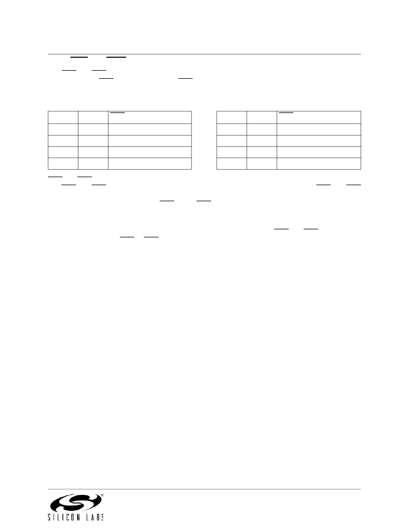
�16.3.� INT0� and� INT1� External� Interrupt� Sources�
�The� INT0� and� INT1� external� interrupt� sources� are� configurable� as� active� high� or� low,� edge� or� level� sensi-�
�tive.� The� IN0PL� (INT0� Polarity)� and� IN1PL� (INT1� Polarity)� bits� in� the� IT01CF� register� select� active� high� or�
�active� low;� the� IT0� and� IT1� bits� in� TCON� (Section� “26.1.� Timer� 0� and� Timer� 1”� on� page� 266)� select� level� or�
�edge� sensitive.� The� table� below� lists� the� possible� configurations.�
�IT0�
�1�
�1�
�0�
�0�
�IN0PL�
�0�
�1�
�0�
�1�
�INT0� Interrupt�
�Active� low,� edge� sensitive�
�Active� high,� edge� sensitive�
�Active� low,� level� sensitive�
�Active� high,� level� sensitive�
�IT1�
�1�
�1�
�0�
�0�
�IN1PL�
�0�
�1�
�0�
�1�
�INT1� Interrupt�
�Active� low,� edge� sensitive�
�Active� high,� edge� sensitive�
�Active� low,� level� sensitive�
�Active� high,� level� sensitive�
�INT0� and� INT1� are� assigned� to� Port� pins� as� defined� in� the� IT01CF� register� (see� SFR� Definition� 16.7).� Note�
�that� INT0� and� INT0� Port� pin� assignments� are� independent� of� any� Crossbar� assignments.� INT0� and� INT1�
�will� monitor� their� assigned� Port� pins� without� disturbing� the� peripheral� that� was� assigned� the� Port� pin� via� the�
�Crossbar.� To� assign� a� Port� pin� only� to� INT0� and/or� INT1,� configure� the� Crossbar� to� skip� the� selected� pin(s).�
�This� is� accomplished� by� setting� the� associated� bit� in� register� PnSKIP� (see� Section� “20.1.� Priority� Crossbar�
��IE0� (TCON.1)� and� IE1� (TCON.3)� serve� as� the� interrupt-pending� flags� for� the� INT0� and� INT1� external� inter-�
�rupts,� respectively.� If� an� INT0� or� INT1� external� interrupt� is� configured� as� edge-sensitive,� the� corresponding�
�interrupt-pending� flag� is� automatically� cleared� by� the� hardware� when� the� CPU� vectors� to� the� ISR.� When�
�configured� as� level� sensitive,� the� interrupt-pending� flag� remains� logic� 1� while� the� input� is� active� as� defined�
�by� the� corresponding� polarity� bit� (IN0PL� or� IN1PL);� the� flag� remains� logic� 0� while� the� input� is� inactive.� The�
�external� interrupt� source� must� hold� the� input� active� until� the� interrupt� request� is� recognized.� It� must� then�
�deactivate� the� interrupt� request� before� execution� of� the� ISR� completes� or� another� interrupt� request� will� be�
�generated.�
�Rev.� 1.4�
�127�
�发布紧急采购,3分钟左右您将得到回复。
相关PDF资料
C8051F912DK
KIT DEV FOR C8051F91X/C8051F90X
C8051F930-TB
BOARD TARGET/PROTO W/C8051F930
C8051T610DB24
DAUGHTER BOARD T610 24QFN SOCKET
C8051T630DB20
BOARD SOCKET DAUGHTER 20-QFN
CAN-100
BOARD EVAL RS232 100QFP
CANADAPT28
KIT ADAPTER CANDEMOBOARD 28PLCC
CAT24AA01WI-GT3
IC EEPROM SERIAL 1KB I2C 8SOIC
CAT24AA02WI-G
IC EEPROM SERIAL 2KB I2C 8SOIC
相关代理商/技术参数
C8051F381
制造商:SILABS 制造商全称:SILABS 功能描述:USB DRIVER CUSTOMIZATION
C8051F381-GM
功能描述:8位微控制器 -MCU USB-64K-Flash
RoHS:否 制造商:Silicon Labs 核心:8051 处理器系列:C8051F39x 数据总线宽度:8 bit 最大时钟频率:50 MHz 程序存储器大小:16 KB 数据 RAM 大小:1 KB 片上 ADC:Yes 工作电源电压:1.8 V to 3.6 V 工作温度范围:- 40 C to + 105 C 封装 / 箱体:QFN-20 安装风格:SMD/SMT
C8051F381-GMR
功能描述:8位微控制器 -MCU USB-Flash-64k-ADC RoHS:否 制造商:Silicon Labs 核心:8051 处理器系列:C8051F39x 数据总线宽度:8 bit 最大时钟频率:50 MHz 程序存储器大小:16 KB 数据 RAM 大小:1 KB 片上 ADC:Yes 工作电源电压:1.8 V to 3.6 V 工作温度范围:- 40 C to + 105 C 封装 / 箱体:QFN-20 安装风格:SMD/SMT
C8051F381-GQ
功能描述:8位微控制器 -MCU USB-64K-Flash
RoHS:否 制造商:Silicon Labs 核心:8051 处理器系列:C8051F39x 数据总线宽度:8 bit 最大时钟频率:50 MHz 程序存储器大小:16 KB 数据 RAM 大小:1 KB 片上 ADC:Yes 工作电源电压:1.8 V to 3.6 V 工作温度范围:- 40 C to + 105 C 封装 / 箱体:QFN-20 安装风格:SMD/SMT
C8051F381-GQR
功能描述:8位微控制器 -MCU USB-Flash-64k-ADC RoHS:否 制造商:Silicon Labs 核心:8051 处理器系列:C8051F39x 数据总线宽度:8 bit 最大时钟频率:50 MHz 程序存储器大小:16 KB 数据 RAM 大小:1 KB 片上 ADC:Yes 工作电源电压:1.8 V to 3.6 V 工作温度范围:- 40 C to + 105 C 封装 / 箱体:QFN-20 安装风格:SMD/SMT
C8051F382
制造商:SILABS 制造商全称:SILABS 功能描述:USB DRIVER CUSTOMIZATION
C8051F382-GQ
功能描述:8位微控制器 -MCU USB-Flash-32k-ADC
RoHS:否 制造商:Silicon Labs 核心:8051 处理器系列:C8051F39x 数据总线宽度:8 bit 最大时钟频率:50 MHz 程序存储器大小:16 KB 数据 RAM 大小:1 KB 片上 ADC:Yes 工作电源电压:1.8 V to 3.6 V 工作温度范围:- 40 C to + 105 C 封装 / 箱体:QFN-20 安装风格:SMD/SMT
C8051F382-GQR
功能描述:8位微控制器 -MCU USB-Flash-32k-ADC RoHS:否 制造商:Silicon Labs 核心:8051 处理器系列:C8051F39x 数据总线宽度:8 bit 最大时钟频率:50 MHz 程序存储器大小:16 KB 数据 RAM 大小:1 KB 片上 ADC:Yes 工作电源电压:1.8 V to 3.6 V 工作温度范围:- 40 C to + 105 C 封装 / 箱体:QFN-20 安装风格:SMD/SMT